 | –≠–ª–µ–∫—Ç—Ä–æ–Ω–Ω—ã–π –∫–æ–º–ø–æ–Ω–µ–Ω—Ç: EM78860BQ | –°–∫–∞—á–∞—Ç—å:  PDF PDF  ZIP ZIP |

* This specification is subject to be changed without notice.
4.17.2000
EM78P860
8 -BIT MICRO-CONTROLLER
1
I.
GENERAL DESCRIPTION
The EM78P860 is an 8-bit RISC type microprocessor with low power , high speed CMOS technology .
Integrated onto a single chip are on_chip watchdog (WDT) , RAM , ROM , programmable real time clock /counter ,
internal interrupt , power down mode , LCD driver and tri-state I/O . The EM78P860 provides a single chip solution
to design a message display .
II.
FEATURES
CPU
∑ Operating voltage range : 2.5V~5.5V
∑ 16Kx13 on chip ROM
∑ 2.8Kx8 on chip RAM
∑ Up to 32 bi-directional tri-state I/O ports
∑ 8 Level stack for subroutine nesting
∑ 8-bit real time clock/counter (TCC)
∑ Two sets of 8 bit counters can be interrupt sources
∑ Selective signal sources and with overflow interrupt
∑ Programmable free running on chip watchdog timer
∑ 99.9% single instruction cycle commands
∑ Four modes (internal clock 3.679MHz, external 32.768KHz)
1.
Sleep mode : CPU and 3.679MHz clock turn off, 32.768KHz clock turn off
2.
Idle mode : CPU and 3.679MHz clock turn off, 32.768KHz clock turn on
3.
Green mode : 3.679MHz clock turn off, CPU and 32.768KHz clock turn on
4.
Normal mode : 3.679MHz clock turn on , CPU and 32.768KHz clock turn on
∑ Low battery detector
∑ Input port wake up function
∑ 8 interrupt source , 4 external , 3 internal
∑ 100 pin QFP (EM78860AQ, POVD disable) (EM78860BQ, POVD enable) or chip (EM78860H)
∑ Port key scan function
∑ Port interrupt , pull high and open drain functions
∑ Clock frequency 32.768KHz externally
LCD
∑ LCD operation voltage chosen by software
∑ Common driver pins : 16
∑ Segment driver pins : 60
∑ 1/4 bias
∑ 1/8,1/16 duty
III.
APPLICATION
1. adjunct units
EM78P860
8 -BIT MICRO-CONTROLLER
* This specification is subject to be changed without notice.
4.17.2000
2
IV.
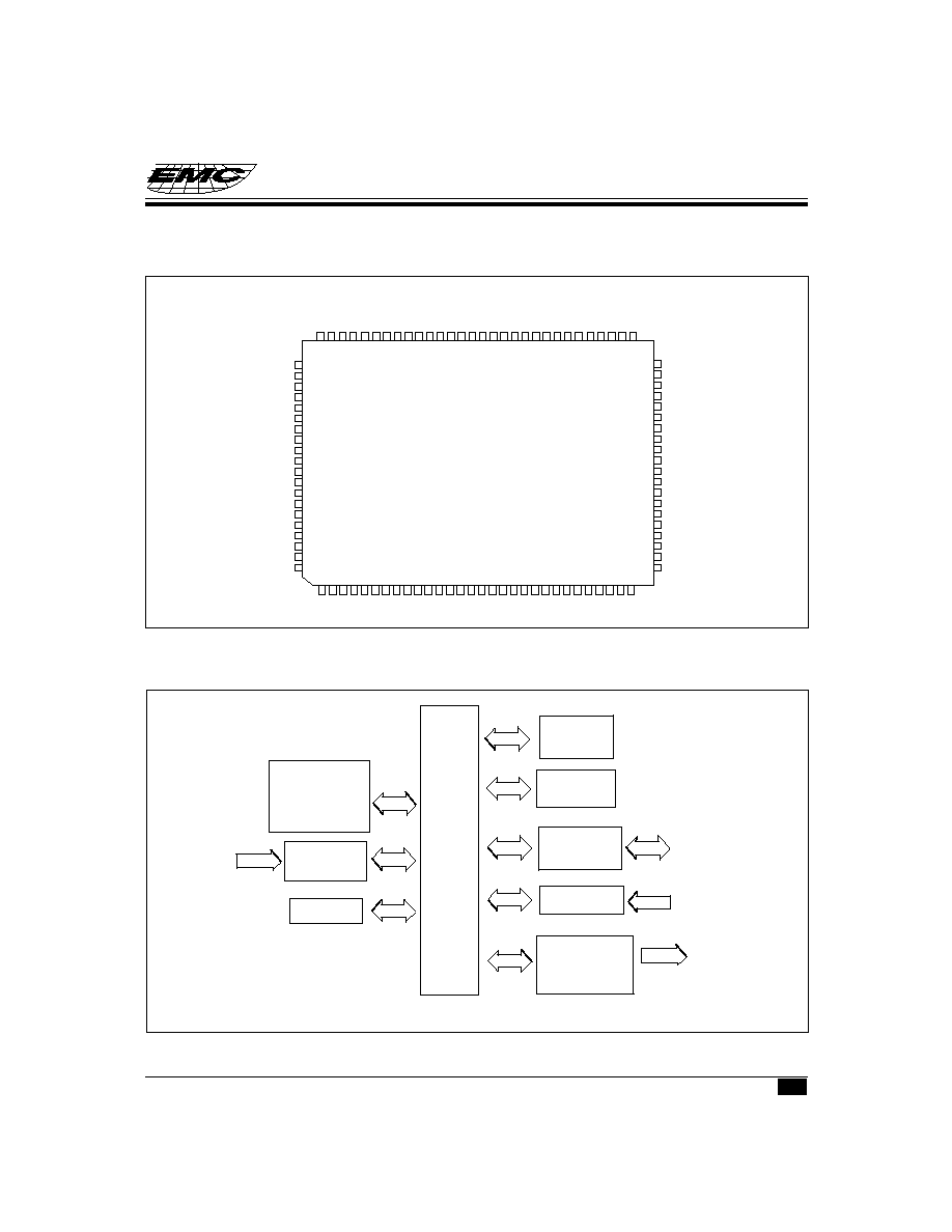
PIN ASSIGNMENTS
ROM
RAM
CPU
INPUT PORT
INPUT PORT
I/O PORT
I/O PORT
LCD
OUTPUT
LCD
LATCH
& DRIVER
CLK
TIMING
CONTROL
TIMER
V.
FUNCTIONAL BLOCK DIAGRAM
SEG42
SEF43
TEST
SEG44/P8.0
SEG45/P8.1
SEG46/P8.2
SEG47/P8.3
SEG48/P8.4
SEG49/P8.5
SEG50/P8.6
SEG51/P8.7
SEG52/P9.0
SEG53/P9.1
SEG54/P9.2
SEG55/P9.3
SEG56/P9.4
SEG57/P9.5
SEG58/P9.6
SEG59/P9.7
VDD1
81
82
83
84
85
86
87
88
89
90
91
92
93
94
95
96
97
98
99
100
80
79
78
77
76
75
74
73
72
71
70
69
68
67
66
65
64
63
62
61
60
59
58
57
56
55
54
53
52
51
GND
NC
PLLC
NC
NC
NC
NC
NC
XIN
XOUT
VDD
SEG0
SEG1
SEG2
SEG3
SEG4
SEG5
SEG6
SEG7
SEG8
SEG9
SEG10
SEG11
SEG12
SEG13
SEG14
SEG15
SEG16
VDD2
SEG17
EM78P860
50
49
48
47
46
45
44
43
42
41
40
39
38
37
36
35
34
33
32
31
1
2
3
4
5
6
7
8
9
10
11
12
13
14
15
16
17
18
19
20
21
22
23
24
25
26
27
28
29
30
COM1
COM0
SEG35
SEG34
SEG33
SEG32
SEG31
SEG30
SEG29
SEG28
SEG27
SEG26
SEG25
SEG24
SEG23
SEG22
SEG21
SEG20
SEG19
SEG18
SEG41
SEG40
SEG39
SEG38
SEG37
SEG36
RESET
P7.7
P7.6
P7.5
P7.4
P7.3/INT3
P7.2/INT2
P7.1/INT1
P7.0/INT0
COM15/P6.7
COM14/P6.6
COM13/P6.5
COM12/P6.4
COM11/P6.3
COM10/P6.2
COM9/P6.1
COM8/P6.0
COM7
COM6
COM5
COM4
COM3
GND
COM2
Fig. 1 Pin assignments
Fig. 2 Functional block diagram1
* This specification is subject to be changed without notice.
4.17.2000
EM78P860
8 -BIT MICRO-CONTROLLER
3
WDT Timer
Control of
sleep and
wake-up
on I/O ports
IOC6
R6
PORT6
Instruction
Decoder
ROM
Interrupt
Controller
R1(TCC)
Oscillator/Timing
Control
Prescaler
RAM
R4
Instruction
register
R2
Stack
XIN
XOUT
DATA & CONTROL BUS
2.5K RAM
ACC
R3
R5
ALU
GENERAL
RAM
P60~P67
IOC7
R7
PORT7
P70~P77
IOC8
R8
PORT8
P80~P87
IOC9
R9
PORT9
P90~P97
VI.
PIN DESCRIPTIONS
Symbol
Type
Function
VDD
POWER
Power
GND
POWER
Gound
XTin
I
Input pin for 32.768 kHz oscillator
XTout
O
Output pin for 32.768 kHz oscillator
PLLC
I
Phase loop lock capacitor, connect a capacitor 0.01
µ
to 0.047
µ
with GND
COM0..COM7
O
Common driver pins of LCD drivers
COM8..COM15
O (PORT6)
SEG0..SEG43
Segment driver pins of LCD drivers
SEG44..SEG51
O (PORT8)
SEG52..SEG59
O (PORT9)
PORT9 AS FUNCTION KEY CAN WAKE UP WATCHDOG.
INT0
PORT7(0)
PORT7(0)~PORT7(3) signal can be interrupt signals.
INT1
PORT7(1)
INT2
PORT7(2)
INT3
PORT7(3)
P7.0~P7.7
PORT7
PORT 7 can be INPUT or OUTPUT port each bit.
Internal Pull high function.
Key scan function.
Bit6,7 open drain function.
P6.0~P6.7
PORT6
PORT 6 can be INPUT or OUTPUT port each bit.
And shared with Common signal.
P8.0~P8.7
PORT8
PORT 8 can be INPUT or OUTPUT port each bit.
And shared with Common signal.
P9.0~P9.7
PORT9
PORT 9 can be INPUT or OUTPUT port each bit.
And shared with Common signal.
TEST
I
Test pin into test mode , normal low
RESET
I
Fig. 2 Functional block diagram2
EM78P860
8 -BIT MICRO-CONTROLLER
* This specification is subject to be changed without notice.
4.17.2000
4
VII. FUNCTION DESCRIPTION
VII.1
Operational Registers
1. R0 (Indirect Addressing Register)
R0 is not a physically implemented register. It is useful as indirect addressing pointer. Any instruction using R0 as
register actually accesses data pointed by the RAM Select Register (R4).
2.
R1 (TCC)
∑ Increased by an internal signal edge applied to TCC , or by the instruction cycle clock.
∑ Written and read by the program as any other register.
3.
R2 (Program Counter)
∑ The structure is depicted in Fig. 4.
∑ Generates 16Kx13 on-chip ROM addresses to the relative programming instruction codes.
∑ "JMP" instruction allows the direct loading of the low 10 program counter bits.
∑ "CALL" instruction loads the low 10 bits of the PC, PC+1, and then push into the stack..
∑ "RET'' ("RETL k", "RETI") instruction loads the program counter with the contents at the top of stack.
∑ "MOV R2,A" allows the loading of an address from the A register to the PC, and the ninth and tenth bits are cleared
to "0''.
∑ "ADD R2,A" allows a relative address be added to the current PC, and contents of the ninth and tenth bits are
cleared to "0''.
∑ "TBL" allows a relative address be added to the current PC, and contents of the ninth and tenth bits don't change.
∑ The most significant bit (A10~A13) will be loaded with the content ofbit PS0~PS3 in the status register (R5)
upon the execution of a "JMP'', "CALL'', "ADD R2,A'', or "MOV R2,A'' instruction.
Fig. 4 Program counter organization
PC
A13 A12 A11 A10
A9 A8
RET
RETTL
RETI
CALL
A7~A0
Stack 1
Stack 2
Stack 3
Stack 4
Stack 5
Stack 6
Stack 7
Stack 8
0000 PAGE0 0000~03FF
0000 PAGE1 0400~07FF
1110 PAGE14 3800~3BFF
1111 PAGE15 3C00~3FFF
0000 PAGE2 0800~0BFF
* This specification is subject to be changed without notice.
4.17.2000
EM78P860
8 -BIT MICRO-CONTROLLER
5
EVENT
T
P
REMARK
WDT TIME OUT
0
0
sleep mode
WDT time out (not sleep mode
0
1
/RESET wake up from sleep
1
0
power up
1
1
Low pulse on /RESET
x
x
x . . don't care
R0
R1(TCC)
R2(PC)
R3(STATUS)
R4(RSR)
R5(ROM PAGE)
R6(PORT6)
R7(PORT7)
R8(PORT8)
R9(PORT9)
RA(CLK)
RB()
RC(2.5K RAM ADRESS)
RD(2.5K RAM DATA)
RE
RF(INT FLAG)
00
01
02
03
04
05
06
07
08
09
0A
0B
0C
0D
0E
0F
10
:
1F
20
:
3F
16x8
Common
Register
IOC6
IOC7
IOC8
IOC9
IOCA
IOCB(LCD ADDRESS)
IOCC(LCD DATA)
IOCD(PULL HIGH)
IOCE(IO, LCD)
IOCF(INT CONTROL)
RC(ADDRESS) RD(DATA)
IOCB(COUNTER1)
IOCC(COUNTER2)
BANK0~BANK3
32X8 ~ 32X8
REGISTER
0
:
255
BAND1
256X8
BAND1
256X8
BAND10
256X8
page0
page1
. . . . . . . . . . . .
. . . . . . . . . . . .
ADDRESS REGISTER
CONTROL REGISTER
(PAGE0)
CONTROL REGISTER
(PAGE1)
4.
R3 ( Status Register )
7
6
5
4
3
2
1
0
-
PAGE
-
T
P
Z
DC
C
∑ Bit 0 (C) :
Carry flag
∑ Bit 1 (DC) :
Auxiliary carry flag
∑ Bit 2 (Z) :
Zero flag
∑ Bit 3 (P) :
Power down bit. Set to 1 during power on or by a "WDTC" command and reset to 0 by a "SLEP"
command.
∑ Bit 4 (T) :
Time-out bit. Set to 1 by the "SLEP" and "WDTC" command, or during power up and reset to 0 by
WDT time out.
∑ Bit 5 : unused
∑ Bit 6 PAGE : changed IOCB~IOCE to another page, 0/1
page0/page1
∑ Bit 7 unused
Fig. 5 Data memory configuration